The shrinking size of features on modern processors is slowly approaching a limit where the wiring on chips will only be a few atoms across. As this point approaches, both making these features and controlling the flow of current through them becomes a serious challenge, one that bumps up against basic limits of materials.
During my visit to IBM's Watson Research Center, it was clear that people in the company are already thinking about what to do when they run into these limits. For at least some of them, the answer would involve a radical departure from traditional chipmaking approaches, switching from traditional semiconductors to carbon nanotubes. And, while I was there, the team was preparing a paper (now released by Nature Nanotechnology) that would report some significant progress: a chip with 10,000 working transistors made from nanotubes, formed at a density that's two orders of magnitude higher than any previously reported effort.
During my visit to Watson, I spoke with George Tulevski, who is working on the nanotube project, and is one of the authors of the recent paper. Tulevski described nanotubes as a radical rethinking of how you build a chip. "Silicon is a solid you carve down," he told Ars, "while nanotubes are something you have to build up." In other words, you can't start with a sheet of nanotubes and etch them until you're left with the wiring you want.
One possible alternative is to use graphene, a sheet of carbon a bit like an unrolled nanotube, which can potentially be etched into distinct features. The problem, according to Tulevski, is that graphene doesn't naturally have a bandgap, the feature of semiconductors that makes them useful for circuitry. It's possible to manipulate graphene so that it develops a bandgap, but that adds to the complexity of manufacturing devices. Some carbon nanotubes, in contrast, are semiconductors without the need for any manipulation (others are metals).
This still left IBM with a choice, Tulevski said. You could potentially attempt to grow a pure population of carbon nanotubes in place, on your chip. We've gotten much better at controlling the growth of nanotubes, and IBM has equipment in house that be used to produce them. The problem there is that, if anything goes wrong with just one of the tubes, the whole chip would be lost. We may have gotten much better, but we've not gotten that good.
So, Tulevski's group is taking a different approach: buy off-the-shelf nanotubes, isolate the ones they want, and then assemble them on a chip.
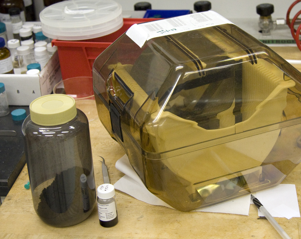
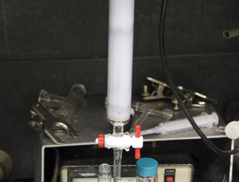
The first couple of steps of this is easier than it sounds. Tulevski showed off a large jar, obtained from a chemical manufacturer, that contained a mixture of carbon nanotubes. As it turns out, the two types of nanotubes, metals and semiconductors, interact differently with a standard column of the type commonly used in chemistry and biochemistry labs. Simply run a mixture down the column, and it's possible to separate out a relatively pure population of one type. To make matters even more convenient, the two populations are slightly different colors.
Once you have a collection of semiconducting nanotubes, you have to build circuits out of these. If we're ever going to make processors out of them, this has to be done quickly, cheaply, and consistently. As Tulevsky described it in referring to purifying the right nanotubes, a one part-per-billion error rate just isn't good enough when you consider the number of transistors on a modern chip.
The team at Watson is working on solution processing, which is where the new paper comes in. The idea is to pre-pattern the needed circuitry onto a chip using IBM's existing foundry experience. Once that's in place, a solution containing carbon nanotubes can be washed across the chip, at which point they'll drop out of solution and attach to the chip based on the pattern.
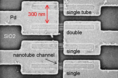
In the paper, the pattern was set up by etching away silicon dioxide to reveal an underlying layer of hafnium dioxide. The HfO2 layer could interact with a charged organic molecule (4-(N-hydroxycarboxamido)-1-methylpyridinium iodide), creating a charged surface. The carbon nanotubes could then be floated across this surface while encased in a coating of an organic molecule with the opposite charge. A simple ion exchange reaction locks the nanotube in place above the hafnium layer.
With the hafnium features at 70nm wide, this process was used to create field-effect transistors (FETs), and it worked with an efficiency of over 90 percent. The density of these FETs was 109 per square centimeter, 100 times higher than the previous reported best. And these devices could be made en masse: the researchers were able to test over 10,000 of the FETs on a single chip, and found over 7,000 functional ones (most of the rest ended up with a metallic nanotube instead of a semiconductor).
This still isn't ready for chip manufacture. But it's a lot closer than most previous efforts, and gives IBM's team some obvious things to troubleshoot if they want to boost the efficiency further.
No comments:
Post a Comment